
The Chip the World Forgot
or Why Mature Semiconductors Are the Most Contested Terrain in the Technology War

Control over the leading edge
There is a geography of attention in the semiconductor industry, and it runs almost entirely in one direction. Every earnings call, every policy announcement, every analyst note gravitates toward the frontier: the 3nm, the 2nm, the gate-all-around transistor architectures that TSMC, Samsung, and Intel race to commercialize at the cost of tens of billions per node. This is the narrative of the technology war as most people understand it, and it is not wrong, exactly. Control over the leading edge matters enormously for the future of artificial intelligence, high-performance computing, and the processors that will define the next decade of digital infrastructure.
But this narrative carries a structural blind spot, one that becomes visible only when supply chains fail, when a car plant shuts down for want of a forty-dollar chip, when a missile guidance system depends on a process node that no one has invested in for years. The chips that run the physical economy are not the chips that make headlines.
They are fabricated at 28 nanometers, at 40nm, at 65nm, at 90nm.
They are produced in foundries that no retail investor could name, using equipment that ASML does not bother to advertise. They are the unspectacular infrastructure beneath the spectacle, and they are increasingly the most contested terrain in the global technology war.
The argument of this analysis is precise: the semiconductor industry has misallocated its narrative resources. Mature nodes, defined here as 28nm and above, represent the largest share of foundry revenue by volume, underpin the most strategically sensitive applications in the real economy, and are the segment where China has made the most material progress under Western export controls.
The geopolitical implications are more immediate than the battle for the leading edge. The investment implications are so, underpriced.
I. The Taxonomy of Invisibility
To understand why mature nodes have been ignored, it is necessary to understand how the industry narrates itself.
The semiconductor industry is organized around a performance hierarchy that doubles as a prestige hierarchy. Each new node generation, defined loosely by gate length, represents a reduction in transistor size, an increase in density, an improvement in power efficiency.

Moore’s Law, the observation that transistor counts double approximately every two years, became an industry ideology. Foundries competed not merely on economic terms but on the symbolic capital of being first to a new node. TSMC’s dominance was understood as a function of its process leadership, its ability to print circuits smaller and faster than anyone else.
This framework is technically coherent for a specific category of chips: the logic processors, graphics accelerators, and neural network inference engines that power cloud computing, artificial intelligence, and high-end mobile devices. For these applications, process shrinkage translates directly into performance and efficiency gains that justify the premium. A data center running NVIDIA H100s running at 4nm versus an older generation at 7nm is not a marginal improvement. It is an architectural discontinuity.
But this framework describes, at most, a minority of the semiconductor market by unit volume, and a segment of the market that does not correspond to the applications most sensitive to supply chain disruption. The physical economy, the economy of automobiles and industrial equipment and power grids and medical devices and military systems, runs on a different class of silicon entirely.
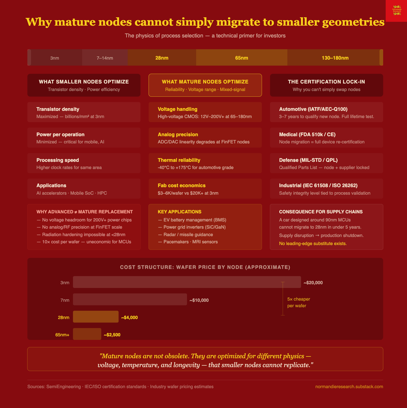
Automotive electronics require chips that can tolerate temperature swings from -40°C to +150°C, survive vibration for a decade or more, and meet functional safety certifications that take years to obtain. These constraints are not compatible with aggressive node scaling. A microcontroller managing an electric vehicle’s battery management system does not need to be fabricated at 3nm.
It needs to be fabricated at a process node with a proven long-term reliability record, stable supply, and a design ecosystem that automotive engineers understand. That node is typically somewhere between 28nm and 180nm.
The same logic applies to industrial automation, where control systems run for fifteen to twenty years without replacement. It applies to aerospace and defense, where radiation tolerance and long qualification cycles make legacy nodes not merely acceptable but mandatory. It applies to power semiconductors, silicon carbide and gallium nitride devices for energy conversion and motor control, which are manufactured at mature nodes where the physics of wide-bandgap materials are best understood. It applies to medical devices, where regulatory approval cycles mean that a chip qualified at 90nm in 2010 may still be the only certifiable option for a pacemaker in 2025.
The result is a structural bifurcation that the industry’s dominant narrative has failed to adequately theorize.
At one end: a small number of chips, produced in very small volumes, at the absolute frontier of what physics and engineering permit, commanding extraordinary margins and requiring extraordinary capital.
At the other: an enormous number of chips, produced in massive volumes, at nodes that a first-year engineering student might describe as obsolete, underpinning applications that cannot function without them, and whose production geography has received almost no strategic attention until supply chains began to fail.
II. The Real Economy of Silicon
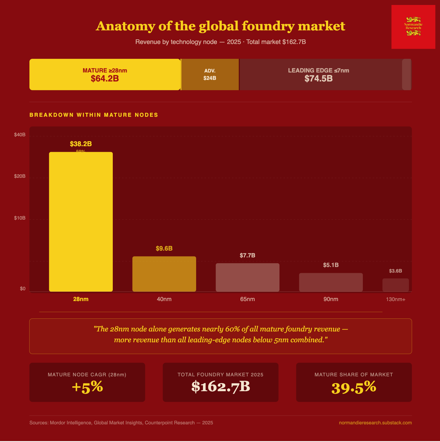
The scale of mature node production is not widely appreciated. According to market data compiled through 2025, the 28nm node alone accounted for roughly 59% of total semiconductor foundry revenue, a figure that reflects not the margin premium of leading-edge silicon but the sheer volume of chips the real economy consumes at this level. Total mature node revenue, at 28nm and above, reached approximately $64.2 billion in 2025, representing the largest single segment of the $162.7 billion global foundry market.
This is not a niche: it is the center of mass.
The application map of mature nodes runs across every sector that matters for physical industrial output. Microcontrollers, the chips that provide basic computational intelligence to embedded systems, are manufactured across a wide range of nodes from 28nm to 180nm and are present in virtually every electromechanical system produced at scale.
A modern automobile contains somewhere between 1,000 and 3,000 discrete semiconductors, with the majority fabricated at mature nodes. The automotive sector’s acute vulnerability became apparent during the pandemic-era chip shortage of 2020-2021, when the U.S. Department of Commerce confirmed that firms faced their most acute shortages specifically at the 40nm node and larger. Assembly lines at Ford, GM, and Volkswagen halted not because of a shortage of cutting-edge processors but because a $2 microcontroller managing a power window was unavailable.
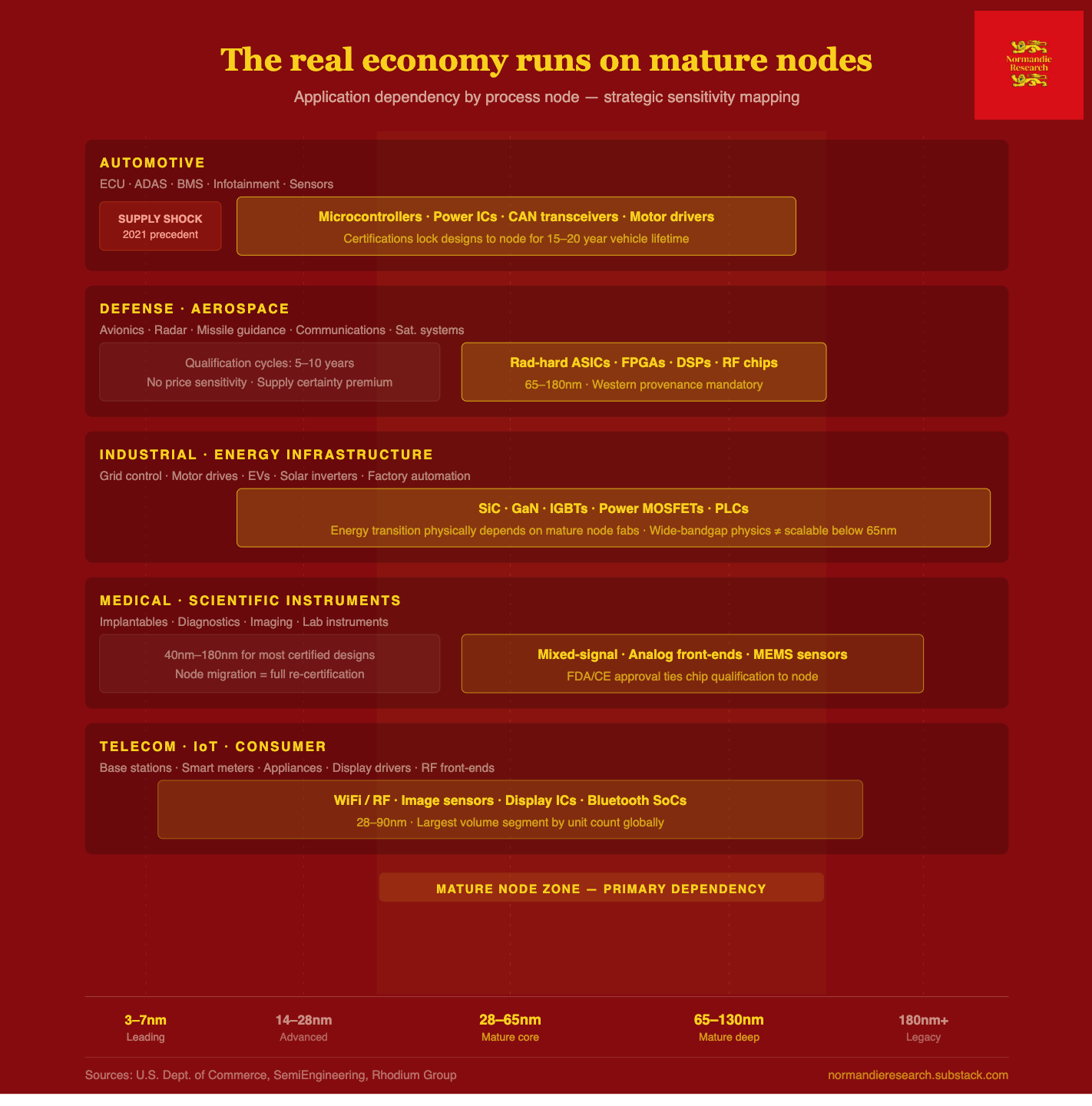
Defense applications add a layer of strategic sensitivity that makes the automotive case look simple. Military electronics, avionics, radar systems, missile guidance, communication infrastructure, operate under constraints that are essentially incompatible with leading-edge node migration. The reliability and radiation-hardness requirements for military-grade components typically translate to process nodes between 65nm and 180nm.
The certification and qualification cycles for defense electronics mean that a chip designed at a specific node must be available from a qualified supplier for decades. When that supplier is a Taiwanese or Chinese foundry, the geopolitical exposure is not theoretical. It is structural.
Power semiconductors represent a third category of strategic importance that is almost entirely mature-node dependent. Silicon carbide devices for electric vehicle inverters and industrial motor drives, gallium nitride chips for RF power amplifiers and fast charging systems, insulated-gate bipolar transistors for grid-scale power conversion, all of these are manufactured using process nodes at 65nm and above, and in many cases at 150nm and 200mm wafer sizes. The energy transition, as a physical infrastructure project, depends on mature node fabs in ways that no amount of 2nm TSMC capacity can resolve.

Analog and mixed-signal chips, the interface layer between the digital world and physical reality, operate under yet another set of constraints. Temperature sensors, pressure transducers, motor controllers, power management ICs, all of these require process nodes optimized for voltage handling and analog precision rather than transistor density.
The physics of analog design do not scale with Moore’s Law. A power management chip that must handle 200 volts cannot be meaningfully miniaturized at 3nm. It runs at 65nm or 130nm or older, on process technology that is well-characterized and unlikely to change.
The aggregate picture is of an industrial economy whose silicon dependency is concentrated not at the frontier but at the base. The conversation about semiconductor sovereignty that has dominated policy circles since 2022 has been disproportionately organized around leading-edge production, for understandable reasons, but in ways that may have systematically underweighted the more immediate vulnerabilities.
III. The Geography of Control, and How It Is Shifting
The current geography of mature node production is the product of three decades of supply chain optimization that prioritized cost efficiency over resilience, and which has produced a concentration of capacity in Asia that is now widely understood to be a strategic liability.
Taiwan has historically been the dominant producer of mature node chips, with roughly 44% of the global mature chip market as of 2023, according to industry data from SEMI. This concentration reflects TSMC’s historical willingness to produce at all nodes, not merely the leading edge, and the cluster of secondary Taiwanese foundries, United Microelectronics Corporation most prominently, that built their businesses in the mature segment that TSMC increasingly chose to de-emphasize.
UMC’s position deserves specific attention. Formerly the largest producer of mature-node chips globally before SMIC’s recent expansion, UMC operates across Taiwan, Singapore, Japan, and China. Its 22/28nm to 40nm range accounts for approximately half of its wafer sales by volume.
The company has, in recent years, pursued a deliberate strategy of moving toward specialty and high-voltage CMOS processes as a way to differentiate from price competition in commoditized mature nodes, a rational response to the structural challenge that Chinese capacity expansion now represents for every non-Chinese foundry in this segment.
China’s trajectory in mature nodes is the central geopolitical development of the past three years, and it has received less analytical attention than its significance warrants.
Blocked from accessing extreme ultraviolet lithography equipment by Dutch export controls coordinated with U.S. pressure, and unable to scale advanced node production for reasons that are now structural rather than merely cyclical, Chinese foundries have redirected capital at an extraordinary pace toward mature node capacity. SMIC has ramped new fabs in Lingang and Beijing, with the Beijing facility targeting 28nm to 40nm production. HuaHong Group and NexChip have followed similar trajectories.
The aggregate effect is measurable: China’s share of global mature process foundry capacity stood at 33% in 2024 and is projected by TrendForce to reach 45% by 2027. This is not a marginal shift.
It represents China becoming the dominant global producer of the chips that run the physical economy, a position achieved not through leading-edge breakthroughs but through subsidized, state-directed industrial policy executed with unusual speed and discipline.
The subsidy apparatus supporting this expansion is substantial. Chinese foundries operating at or below 28nm benefit from five-year income-tax holidays followed by reduced tax brackets. Shanghai’s Lingang New Area alone targeted semiconductor output of CNY 100 billion by 2025 through bonded-zone incentives.
Total fiscal support for semiconductor manufacturing between 2020 and 2024 has been estimated at the equivalent of $322 billion, a figure that comprehensively undercuts the economics of unsubsidized competitors in Taiwan, the United States, and Europe.
The pricing consequences are already visible. Chinese foundries recovering faster than their multinational peers have introduced significant downward pressure on mature node pricing.
Capacity utilization for mature nodes among global foundries remained below 80% through much of 2024, with pricing described by TrendForce as remaining “under pressure.”
For UMC and GlobalFoundries, whose business models depend on the economic viability of mature node production in non-Chinese geographies, this is not an abstract competitive threat.
It is a direct challenge to their cost structures.
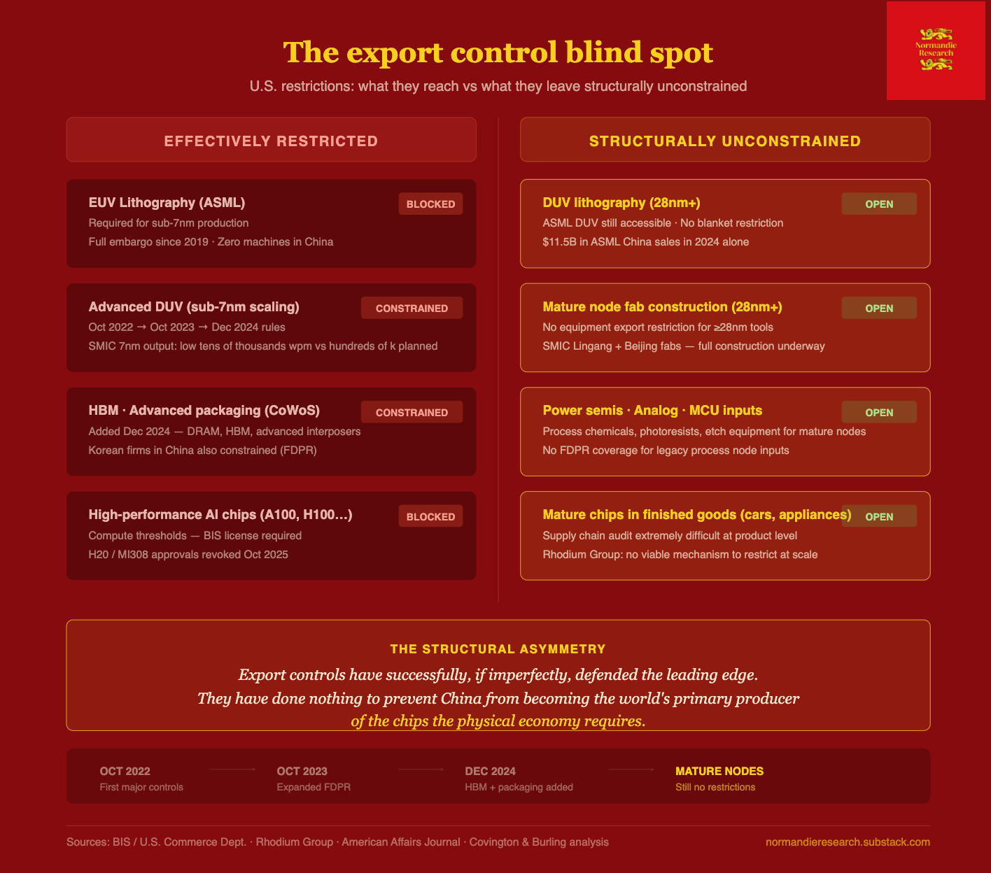
The Western response to this dynamic has been mostly reactive and partially incoherent. Export controls have focused heavily on advanced manufacturing equipment, denying China access to EUV and tightening restrictions on deep ultraviolet lithography. These controls have meaningfully constrained China’s ability to reach sub-7nm production at scale: SMIC’s 7nm output, produced using multi-patterning DUV techniques, remains limited to the low tens of thousands of wafers per month rather than the hundreds of thousands originally planned, according to analysis by Gregory Allen for the Center for Strategic and International Studies. But these same controls do nothing to constrain mature node expansion, which requires only equipment that China can already source or is rapidly developing domestically.
The asymmetry is strategic. Export controls have successfully, if imperfectly, defended the leading edge. They have done nothing to prevent China from positioning itself as the world’s primary producer of the chips the physical economy requires.
IV. The Consolidation Thesis
The most significant near-term development in the mature node industry is the reported merger exploration between GlobalFoundries and United Microelectronics Corporation, first surfaced by Nikkei Asia in early 2025. If completed, the combination would create the world’s second-largest foundry by revenue at approximately $3.7 billion based on Q4 2024 figures, surpassing Samsung Foundry, and would assemble a geographically diversified platform spanning the United States, Germany, Singapore, Taiwan, and Japan.

The strategic logic of the combination is legible precisely because of the mature node dynamics described above. GlobalFoundries, which received $1.5 billion in U.S. government funding in February 2024, specializes in 12nm to 90nm specialty and government-sensitive manufacturing, with clients including Qualcomm, General Motors, and Lockheed Martin. UMC focuses on 22nm to 40nm and has been pushed toward high-voltage specialty processes to resist commodity price competition.
Together, they would have sufficient scale to absorb the pricing pressure from Chinese expansion, sufficient geographic diversification to serve both U.S. and European industrial supply chains, and sufficient defense exposure to attract continued sovereign funding.
The complications are also significant. GlobalFoundries, valued at approximately $20 billion, would need to mobilize substantial capital, potentially from its primary sovereign shareholder Mubadala Investment Company, the Abu Dhabi wealth fund.
Taiwan’s regulatory position is uncertain: Taiwanese authorities may resist foreign control of UMC for the same reasons they have been cautious about TSMC’s overseas expansions. China’s antitrust approval is a separate variable, since UMC operates a fab in China producing 25,000 wafers per month, and Beijing’s willingness to approve a combination that explicitly positions itself as a Western counterweight to SMIC is not obvious.
The merger may not happen.
But the fact that it is being seriously explored is itself diagnostic. It signals that the two most significant non-TSMC, non-Samsung mature node foundries have concluded that their independent scale is insufficient to compete sustainably against subsidized Chinese capacity. The mature node segment is, in other words, already in a consolidation phase driven by geopolitical economics.
V. The Export Control Frontier
The U.S. regulatory approach to mature nodes remains the most uncertain variable in the strategic picture. The Biden administration’s export control packages of 2022, 2023, and December 2024 focused primarily on advanced manufacturing equipment, high-bandwidth memory, and specific entity-list restrictions. They did not impose restrictions on mature node production inputs in the way they have constrained leading-edge equipment.
This is now an active policy debate.
A Rhodium Group analysis identified the potential for significant economic harm from Chinese mature node dominance, particularly in automotive and industrial supply chains, and noted that U.S. options for regulating Chinese legacy chips are constrained by the fact that these chips flow into finished goods through complex supply chains that are difficult to audit.
A Congressional Research Service report on export controls, updated through 2025, notes that restrictions have been progressively expanded but continue to focus on advanced computing and semiconductor manufacturing items, with legacy chips representing a largely unaddressed exposure.
The Trump administration’s approach to this question carries its own complexity. Tariffs on Chinese-manufactured semiconductors are a blunt instrument that increases costs for U.S. manufacturers who depend on mature node chips from Chinese or Chinese-adjacent sources, without necessarily redirecting production to U.S. fabs that have neither the capacity nor the cost structure to absorb this demand rapidly.
The alternative, directly subsidizing Western mature node capacity through CHIPS Act mechanisms, has been partially pursued through the GlobalFoundries grant, but the scale of subsidy required to offset Chinese state support is larger than current U.S. policy has committed.
The European dimension adds a further layer. Europe’s industrial base, automotive in Germany and the Nordics, industrial equipment in Germany and Switzerland, aerospace in France and the UK, is among the most exposed to mature node supply chain concentration. The European Chips Act, passed in 2023, included provisions for mature node production but has been criticized for insufficient scale and ambiguous implementation. The Intel fab project in Germany, designed partly to address leading-edge gap, is also facing financing uncertainty. European mature node sovereignty remains largely aspirational.
VI. Structural Implications
The analysis above converges on a set of structural observations that have not been adequately priced by either policy or markets.
The first is that mature node geopolitical risk is more immediate than leading-edge geopolitical risk for most of the physical economy. A conflict scenario affecting Taiwan would disrupt both TSMC’s advanced node production and the mature node production of TSMC’s Kumamoto fab (28nm/22nm, 55,000 wafers monthly) and UMC’s Taiwanese facilities.
But the effects on the physical economy would manifest first through automotive and industrial supply chains, not through data center capacity. The 2021 chip shortage established the empirical baseline for how quickly mature node shortages propagate into manufacturing shutdowns. The geopolitical scenario would be structurally similar but larger in magnitude.
The second is that Chinese mature node expansion is now structurally entrenched. The capacity additions are physical infrastructure. The subsidies are recurring. The domestic design ecosystem in China, increasingly building for domestic foundries to serve electric vehicles, IoT devices, and consumer electronics, is generating the volume pull-through that justifies continued investment. Reversing China’s position from 33% to 45% of global mature node capacity is not a policy problem that can be solved through export controls alone. It would require sustained Western investment at a scale that has not been authorized.
The third is that the GlobalFoundries-UMC consolidation logic, whether or not this specific transaction proceeds, reflects a structural pressure that will drive further consolidation in the non-Chinese mature node sector. The economic model of operating mid-size mature node foundries in high-cost Western geographies against subsidized Chinese competition is challenged at current scale.
Either sovereign support increases substantially, or consolidation accelerates, or several Western mature node producers exit the market, concentrating supply further.
The fourth is that certain mature node applications retain pricing power and structural moat in ways the aggregate data can obscure. Defense and aerospace customers are not price-sensitive in the way automotive tier-two suppliers are. Specialty processes, radiation-hardened nodes, high-voltage CMOS for power management, photonic integrated circuits at mature nodes for datacom and sensing, these represent pockets of differentiated production where Western foundries maintain both technical leadership and contractual relationships that are difficult for Chinese competitors to displace.
GlobalFoundries’ long-term agreements with Lockheed Martin and General Motors represent the structural expression of this dynamic: customers who need supply certainty and Western provenance pay for it.
The fifth, and perhaps most consequential for investors, is that the attention asymmetry between leading-edge and mature nodes creates a valuation anomaly. The companies most exposed to mature node geopolitical dynamics, UMC, GlobalFoundries (private, Mubadala-controlled), and the IDMs that rely on mature node outsourcing, have not been analyzed with the same rigor as TSMC or ASML.
The merger speculation around GF and UMC has moved UMC’s American depositary receipts meaningfully. But the underlying structural thesis, that Western mature node capacity is a strategic asset being systematically undervalued relative to its geopolitical importance, has not been fully arbitraged.
VII. The Analytical Frame
There is a tendency, when covering the technology war, to reach for the most dramatic formulation available.
The chip war narrative has been told primarily as a story about who controls the frontier, who has the most advanced fabs, who can design the most powerful AI accelerators.
This framing is not incorrect.
Leading-edge semiconductor control is a genuine and significant strategic contest.
But the frontier framing systematically underweights what might be called the infrastructure layer of the semiconductor ecosystem, the unglamorous, heavily subscribed, economically essential production of chips that will never appear in a product launch keynote but without which an automobile cannot accelerate, a power grid cannot route electricity, and a military aircraft cannot navigate.
The most contested terrain in the technology war is not, in the end, the 2nm node. It is the 28nm node. It is the question of who produces the chips that run the physical economy, at what cost, under what political conditions, and with what degree of geographic concentration. China has made a deliberate strategic decision to win this question. The West has not yet made a comparably deliberate decision to contest it.
That asymmetry is the most important structural fact in semiconductor geopolitics that most analysts are not writing about.
Normandie Research is an independent publication producing strategic analysis at the intersection of geopolitics, economic statecraft, capital flows, and financial markets. This analysis is provided for informational purposes only and does not constitute investment advice or a solicitation to buy or sell any financial instrument. Readers should conduct their own due diligence and consult qualified financial advisers before making any investment decision.
This is one of the best pieces of semiconductor analysis ive read this year and the reason is the framing. Everyone writes about the race to 2nm because thats where the prestige is. Nobody writes about the 28nm chips that actually keep the physical world running because theres no narrative energy in a process node that a first-year engineering student would call obsolete.
The 59% revenue share number is the one that should restructure how people think about the entire industry. The leading edge gets the headlines, the capex, the analyst coverage, and the geopolitical attention. The mature nodes get 59% of the revenue and almost none of the strategic planning. Thats a misallocation of attention that has real consequences, as every car manufacturer discovered in 2021 and is discovering again now.
The China angle is the part that genuinely concerns me though. Export controls focused almost entirely on cutting edge access while China built domestic capacity at mature nodes largely unimpeded. If the strategic vulnerability is actually in the chips that run cars, grids, defence systems, and medical devices, then the controls were aimed at the wrong layer. The leading edge is where the prestige is. The mature node is where the leverage is. And right now one country is building capacity at the layer that matters most while everyone else argues about the layer that matters least for the physical economy.